- 您现在的位置:买卖IC网 > Sheet目录490 > NTMD6N03R2 (ON Semiconductor)MOSFET PWR N-CH DL 6A 30V 8SOIC
NTMD6N03R2,
NVMD6N03R2
Power MOSFET
30 V, 6 A, Dual N--Channel SOIC--8
Features
? Designed for use in low voltage, high speed switching applications
http://onsemi.com
? Ultra Low On--Resistance Provides
Higher Efficiency and Extends Battery Life
-- R DS(on) = 0.024 Ω , V GS = 10 V (Typ)
-- R DS(on) = 0.030 Ω , V GS = 4.5 V (Typ)
? Miniature SOIC--8 Surface Mount Package Saves Board Space
V DSS
30 V
R DS(ON) Typ
24 m Ω @ V GS = 10 V
N--Channel
I D Max
6.0 A
?
?
?
?
Diode is Characterized for Use in Bridge Circuits
Diode Exhibits High Speed, with Soft Recovery
AEC Q101 Qualified -- NVMD6N03R2
These Devices are Pb--Free and are RoHS Compliant
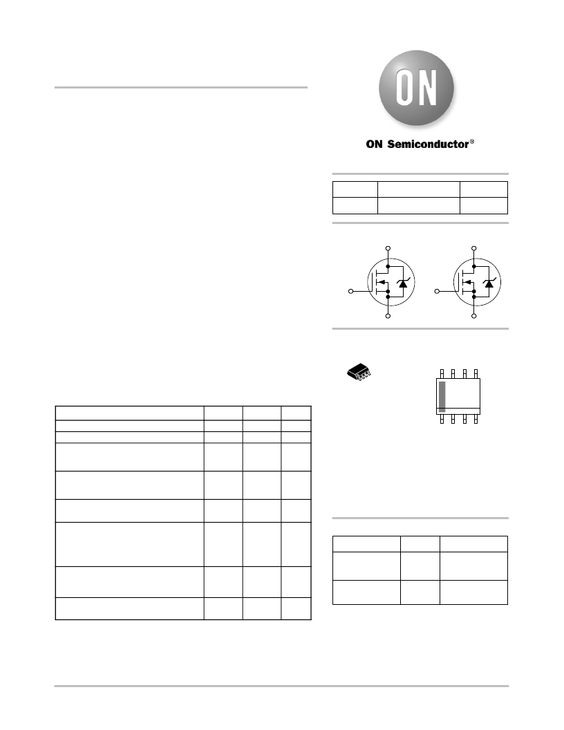
G
D
G
D
Applications
? DC--DC Converters
S
S
?
?
?
?
Computers
Printers
Cellular and Cordless Phones
Disk Drives and Tape Drives
8
1
MARKING DIAGRAM &
PIN ASSIGNMENT
D1 D1 D2 D2
8
E6N03
MAXIMUM RATINGS (T J = 25 ? C unless otherwise noted)
Rating Symbol Value
Drain--to--Source Voltage V DSS 30
Gate--to--Source Voltage -- Continuous V GS ? 20
Unit
Volts
Volts
SOIC--8
CASE 751
STYLE 11
AYWW G
G
1
S1 G1 S2 G2
Drain Current
-- Continuous @ T A = 25 ? C
-- Single Pulse (tp ? 10 m s)
I D
I DM
6.0
30
Adc
Apk
E6N03
A
Y
= Specific Device Code
= Assembly Location
= Year
Total Power Dissipation
@ T A = 25 ? C (Note 1)
@ T A = 25 ? C (Note 2)
Operating and Storage Temperature
Range
Single Pulse Drain--to--Source Avalanche
Energy -- Starting T J = 25 ? C
(V DD = 30 Vdc, V GS = 5.0 Vdc,
V DS = 20 Vdc, Peak I L = 9.0 Apk,
L = 10 mH, R G = 25 Ω )
P D
T J , T stg
E AS
2.0
1.29
--55 to
+150
325
Watts
? C
mJ
WW = Work Week
G = Pb--Free Package
(Note: Microdot may be in either location)
ORDERING INFORMATION
Device Package Shipping ?
NTMD6N03R2G SOIC--8 2500 / Tape &
Thermal Resistance R θ JA ? C/W
-- Junction--to--Ambient (Note 1) 62.5
-- Junction--to--Ambient (Note 2) 97
Maximum Lead Temperature for Soldering T L 260 ? C
Purposes for 10 seconds
Stresses exceeding Maximum Ratings may damage the device. Maximum
Ratings are stress ratings only. Functional operation above the Recommended
Operating Conditions is not implied. Extended exposure to stresses above the
Recommended Operating Conditions may affect device reliability.
1. When surface mounted to an FR4 board using 1 ? pad size, t ? 10 s
2. When surface mounted to an FR4 board using 1 ? pad size, t = steady state
(Pb--Free) Reel
NVMD6N03R2G SOIC--8 2500 / Tape &
(Pb--Free) Reel
?For information on tape and reel specifications,
including part orientation and tape sizes, please
refer to our Tape and Reel Packaging Specification
Brochure, BRD8011/D.
? Semiconductor Components Industries, LLC, 2011
October, 2011 -- Rev. 3
1
Publication Order Number:
NTMD6N03R2/D
发布紧急采购,3分钟左右您将得到回复。
相关PDF资料
NTMD6P02R2G
MOSFET PWR P-CHAN DUAL 20V 8SOIC
NTMFD4901NFT1G
MOSFET N-CH DUAL 30V 8DFN
NTMFS4108NT1G
MOSFET N-CHAN 22A 30V SO-8FL
NTMFS4119NT1G
MOSFET N-CHAN 18A 30V SO-8FL
NTMFS4120NT1G
MOSFET N-CHAN 18A 30V SO-8FL
NTMFS4121NT1G
MOSFET N-CHAN 17A 30V SO-8FL
NTMFS4122NT1G
MOSFET N-CHAN 14A 30V SO-8FL
NTMFS4701NT3G
MOSFET N-CH 12.3A 30V SO8 FL
相关代理商/技术参数
NTMD6N03R2G
功能描述:MOSFET NFET 30V SPCL TR RoHS:否 制造商:STMicroelectronics 晶体管极性:N-Channel 汲极/源极击穿电压:650 V 闸/源击穿电压:25 V 漏极连续电流:130 A 电阻汲极/源极 RDS(导通):0.014 Ohms 配置:Single 最大工作温度: 安装风格:Through Hole 封装 / 箱体:Max247 封装:Tube
NTMD6N04R2
制造商:ONSEMI 制造商全称:ON Semiconductor 功能描述:Power MOSFET 40 V, 5.8 A, Dual N-Channel SOIC-8
NTMD6N04R2G
功能描述:MOSFET NFET SO8 40V 5.8A 0.027R RoHS:否 制造商:STMicroelectronics 晶体管极性:N-Channel 汲极/源极击穿电压:650 V 闸/源击穿电压:25 V 漏极连续电流:130 A 电阻汲极/源极 RDS(导通):0.014 Ohms 配置:Single 最大工作温度: 安装风格:Through Hole 封装 / 箱体:Max247 封装:Tube
NTMD6P02
制造商:ONSEMI 制造商全称:ON Semiconductor 功能描述:Power MOSFET 6 A, 20 V, Pa??Channel SOICa??8, Dual
NTMD6P02R2
功能描述:MOSFET 20V 6A P-Channel RoHS:否 制造商:STMicroelectronics 晶体管极性:N-Channel 汲极/源极击穿电压:650 V 闸/源击穿电压:25 V 漏极连续电流:130 A 电阻汲极/源极 RDS(导通):0.014 Ohms 配置:Single 最大工作温度: 安装风格:Through Hole 封装 / 箱体:Max247 封装:Tube
NTMD6P02R2/D
制造商:未知厂家 制造商全称:未知厂家 功能描述:Power MOSFET 6 Amps, 20 Volts
NTMD6P02R2G
功能描述:MOSFET 20V 6A P-Channel RoHS:否 制造商:STMicroelectronics 晶体管极性:N-Channel 汲极/源极击穿电压:650 V 闸/源击穿电压:25 V 漏极连续电流:130 A 电阻汲极/源极 RDS(导通):0.014 Ohms 配置:Single 最大工作温度: 安装风格:Through Hole 封装 / 箱体:Max247 封装:Tube
NTMD6P02R2SG
功能描述:MOSFET PFET20V 6A .033R TR RoHS:否 制造商:STMicroelectronics 晶体管极性:N-Channel 汲极/源极击穿电压:650 V 闸/源击穿电压:25 V 漏极连续电流:130 A 电阻汲极/源极 RDS(导通):0.014 Ohms 配置:Single 最大工作温度: 安装风格:Through Hole 封装 / 箱体:Max247 封装:Tube
